Technical Specifications
CPU Core: 32-bit internal RISC load-store architecture, SuperH/SH2 compatible instruction set, 16-bit fixed-length instructions.
Registers: Sixteen 32-bit general-purpose registers, three 32-bit control registers, four 32-bit system registers.
Pipeline: Five-stage pipeline with delayed branch support and one basic instruction per clock state.
Clock Frequency: Up to 28.7 MHz maximum operating grade; 35 ns per basic instruction at 28.7 MHz.
Address Space: Up to 4 Gbyte architecture address range; implemented external memory window defined by the bus state controller and board decoding.
Cache Memory: 4 KB on-chip cache, 64 entries, 4-way set associative, 16-byte line, write-through policy, LRU replacement; 2 KB of cache RAM reconfigurable as internal scratch RAM.
Multiplier: 32-bit × 32-bit multiply producing 64-bit result; 32-bit × 32-bit plus 64-bit multiply-accumulate in 2 to 4 states.
Divide Unit: 64-bit ÷ 32-bit and 32-bit ÷ 32-bit operations, execution completed in 39 clock cycles for the standard divide routine, with overflow interrupt.
DMA Controller: Two independent channels; transfer widths 1, 2, 4 or 16 bytes; cycle-steal or burst mode; single or dual address mode; external pin, SCI, timer or auto request sources; maximum 16,777,216 transfers per channel; fixed or round-robin priority.
Timers: One 16-bit free-running timer with internal/external clock selection, input capture and output compare; one watchdog timer switchable as watchdog or interval timer with reset, interrupt or external output.
Serial Interface: One SCI channel, asynchronous or synchronous full-duplex, dedicated baud-rate generator, multiprocessor communication mode.
Interrupt Controller: NMI plus IRL0–IRL3 encoded external inputs providing 15 external vectors; 12 internal sources from DMA, divide, timer, serial and refresh; 16 programmable priority levels; auto-vector or external-vector selection.
Bus State Controller: Four chip-select areas, CS0–CS3, 8/16/32-bit bus width per area, direct interface to DRAM, synchronous DRAM, pseudo-SRAM and burst ROM; RAS/CAS/CE/OE generation, address multiplexing, programmable wait states, DRAM/SDRAM/PSRAM refresh with CAS-before-RAS and self-refresh, burst access support.
Clock Generator: On-chip oscillator/PLL, crystal or external clock input, multiplication ×1/×2/×4, PLL synchronization, 90-degree phase shift option, clock output and clock-pause support.
Debug Unit: User break controller capable of address, data, bus-cycle, instruction/data, read/write and byte/word/long-word break conditions.
Packages: 144-pin plastic QFP, FP-144J; 176-pin plastic TFBGA, TBP-176.
Supply Voltage: 5 V nominal for the standard SH7604 5 V class; absolute maximum VCC −0.3 V to +7.0 V. If the JDVE board uses a different voltage class, confirm the processor marking before power-up.
Operating Temperature: −20 °C to +75 °C standard component operating grade; storage −55 °C to +125 °C. Extended board grading must be taken from the Densan JDVE manual.
Functional Features
Deterministic RISC Execution: Single-state basic instructions, five-stage pipeline and delayed branches for real-time response.
Integrated DSP-Grade Arithmetic: 32×32 multiply and multiply-accumulate for filtering, control loops and signal processing.
Autonomous Data Transfer: Dual-channel DMA moves data between memory, serial, timers and external I/O without continuous CPU intervention.
Glue-Less Memory Interface: Bus state controller connects DRAM, SDRAM, PSRAM and burst ROM directly with programmable timing and refresh.
Flexible Debug And Boot: User break controller, programmable reset states, PLL clock modes and per-area boot memory configuration.
Application Scenarios
Real-Time Industrial Control: PLC support modules, motion controllers, sensor aggregation and actuator supervision.
Embedded Communication Cards: Serial gateways, protocol converters and peripheral management boards.
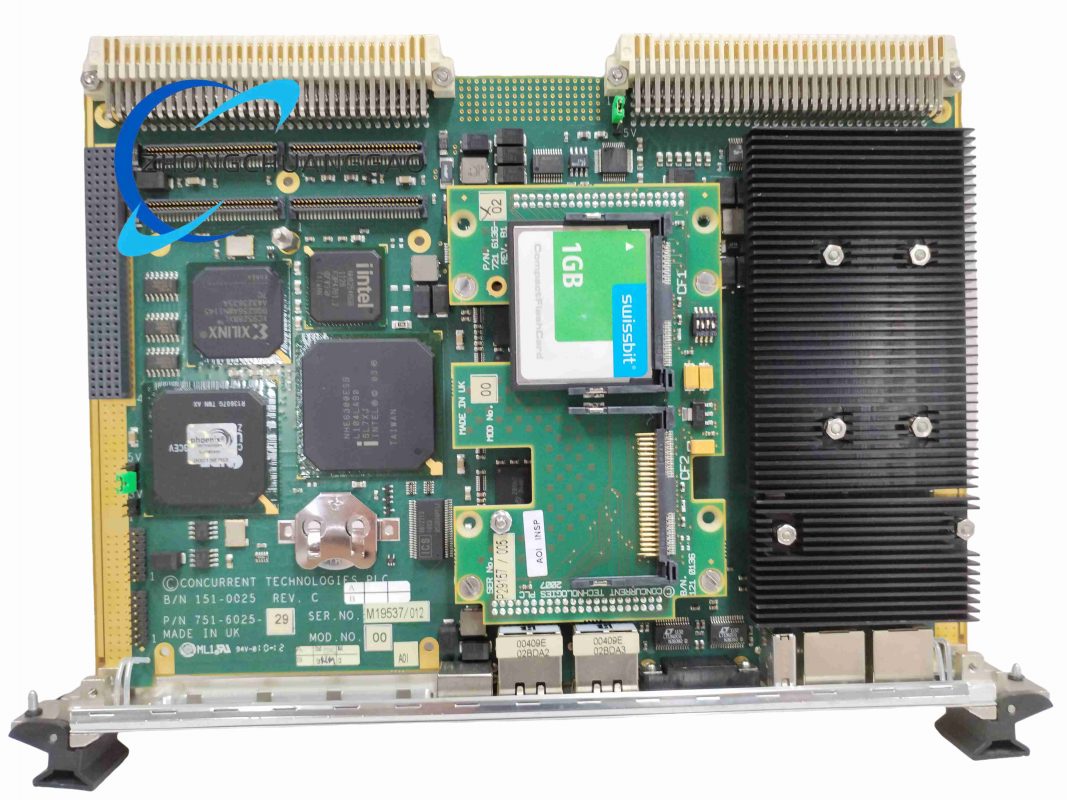
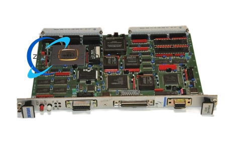
VME Or Backplane SBCs: Boot processor, system monitoring, I/O scheduling and diagnostic control when the JDVE carrier provides the corresponding slot interface.
Test And Instrumentation: Data acquisition front ends, timing modules and low-power RISC compute nodes.
Performance Parameters
Instruction Throughput: One basic RISC instruction per state; 28.57 million basic instructions per second at 28.7 MHz.
Multiply/MAC Latency: Multiply 32×32→64 in 2 to 4 pipeline states; MAC suitable for repeated sum-of-products routines.
Divide Throughput: 64÷32 or 32÷32 completed in 39 clock cycles under the standard divide routine.
DMA Capacity: Up to 16,777,216 programmed transfers per channel with byte, word, long-word or quad-long-word width.
Cache Effect: 16-byte line fill per miss, four-way LRU, write-through consistency; 2 KB cache RAM available for deterministic internal data storage.
Material Composition
Semiconductor Die: CMOS SuperH RISC process.
Package Materials: Plastic QFP or plastic TFBGA encapsulation with lead frame or ball-grid substrate.
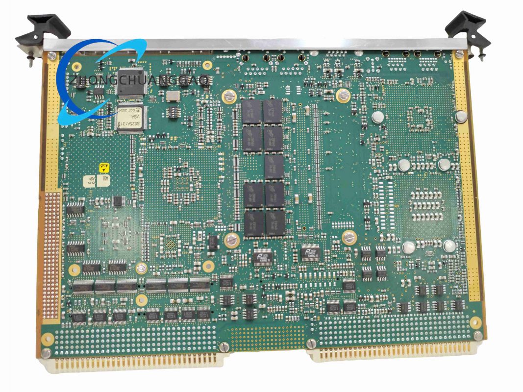
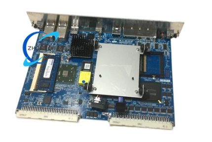
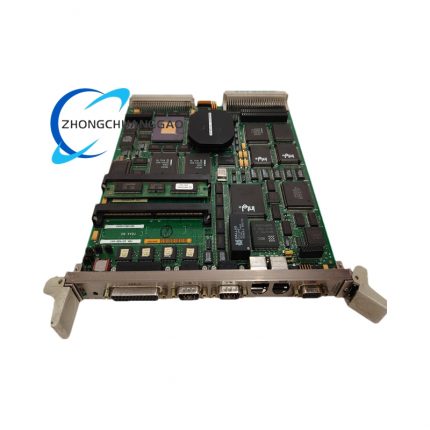
Board Materials: JDVE PCB laminate, voltage regulators, SDRAM/PSRAM/flash devices, serial transceivers, connectors and mechanical hardware are confirmed only from the official Densan JDVE-SH7604 9271 documentation.
Structural Characteristics
Monolithic Microcontroller: CPU, cache, multiplier, divider, DMA, timers, serial, interrupt and bus controller integrated in one device.
External Bus Hierarchy: 32-bit data bus capability with four independent chip-select areas and separate control, address and data pins.
Clock And PLL Domain: Core clock derived from on-chip PLL, external crystal or external oscillator according to mode configuration.
Debug Subsystem: User break controller accessible through emulation tools for address/data/bus-cycle trapping.
Working Principle
The SH7604 fetches 16-bit instructions into the five-stage pipeline, decodes register and memory operations, executes arithmetic, logic, multiply-accumulate or divide in the appropriate functional unit, and writes results to the 32-bit general registers or external memory. The 4 KB cache reduces external memory latency and can be partially reallocated as internal RAM for critical data. DMA channels transfer blocks between memory, SCI, timers and external devices without blocking the CPU. The free-running timer and watchdog generate periodic, capture and safety events. The serial interface performs asynchronous or synchronous communication. The interrupt controller prioritizes NMI, external IRL sources and internal peripherals. The bus state controller converts CPU accesses into DRAM, SDRAM, PSRAM, burst-ROM or I/O control signals using chip-select, RAS/CAS, wait and refresh programming. On the JDVE carrier, the processor boots from the configured chip-select memory, initializes RAM and peripherals, then runs application firmware that manages the board’s I/O and host interface.
Installation Requirements
Power Supply Verification: Confirm 5 V or alternate voltage class from the processor marking and JDVE manual; apply only the rated rail with properly decoupled VCC/GND pairs.
Decoupling Network: Place bypass capacitors on every power/ground pair, separate PLL analog power if required, and maintain low-impedance return paths.
Clock Circuit: Install the crystal, oscillator or external clock specified by the board clock-mode strapping; allow PLL lock time before full-speed operation.
Reset Circuit: Provide power-on reset and manual reset with the pulse width defined in the SH7604 and JDVE hardware manual.
Memory Configuration: Define each bus state controller area for boot ROM, SDRAM/PSRAM, flash and I/O before firmware initialization; set wait states, burst mode and refresh interval.
PCB Assembly: Follow 144-pin QFP or 176-pin TFBGA land patterns, solder-reflow profile and inspection rules; BGA boards require electrical continuity or X-ray validation.
Mechanical Fit: Verify JDVE board format, connector type, mounting holes, heatsink or airflow clearance against the target chassis or backplane.
Usage Precautions
Voltage Compliance: Never exceed absolute maximum VCC −0.3 V to +7.0 V; do not mix 5 V and other voltage-class components.
Pin Handling: Leave reserved, no-connect and unimplemented pins open unless the JDVE manual defines their connection.
Thermal Management: Maintain junction and board temperature within the ordered component and JDVE operating grade; provide forced airflow or heatsinking if the application sustains maximum clock and DMA load.
ESD Protection: Use grounded workbenches, wrist straps and anti-static packaging when handling the processor, memory and board connectors.
Reset And Watchdog: Enable the watchdog in unattended systems; validate boot images and NVRAM or configuration data before field deployment.
Safety Restrictions: Do not deploy the board in life-support, aerospace flight-critical or nuclear safety systems without written Densan qualification and component-level authorization.


-430x381.jpg)



Reviews
There are no reviews yet.