Technical Specifications
CPU Core: 32-bit internal RISC load-store architecture, 16-bit fixed-length instruction set, SH2 compatible.
Pipeline: Five-stage pipeline with one instruction per state for basic operations.
Clock Frequency: Up to 28.7 MHz for the highest-speed verified SH7604 grade; 20 MHz grades exist for lower-power versions.
Cache Memory: 4 KB on-chip cache, 4-way set associative, 64 entries, 16-byte line, write-through policy; part of cache RAM reconfigurable as internal scratch RAM.
Multiplier: 32-bit × 32-bit multiply producing 64-bit result; multiply-accumulate 32-bit × 32-bit plus 64-bit result in 2 to 4 states.
Divide Unit: 64-bit ÷ 32-bit and 32-bit ÷ 32-bit operations with overflow interrupt.
DMA Controller: Two independent channels, transfer widths 1/2/4/16 bytes, cycle-steal or burst mode, auto/internal/external request sources.
Timers: One 16-bit free-running timer with input capture and output compare; one watchdog timer configurable as reset, interrupt or interval source.
Serial Interface: One SCI channel with asynchronous and synchronous full-duplex operation, dedicated baud generator and multiprocessor mode.
Interrupt Controller: NMI plus IRL0–IRL3 encoded external inputs for 15 external vectors, 12 internal sources, 16 programmable priority levels.
Bus Controller: Four chip-select areas, direct interface to DRAM, synchronous DRAM, pseudo-SRAM and burst ROM, 8/16/32-bit bus width per area, programmable wait states and refresh.
Memory Address Space: 4 GB architecture address capability; implemented memory window defined by board design.
Packages: 144-pin plastic QFP and 176-pin plastic TFBGA.
Supply Voltage: 5 V grades operated at 5 V nominal; 3.3 V grades operated at 3.3 V nominal. Exact voltage class must be confirmed from the board label.
Operating Temperature: Standard component grade −20 °C to +75 °C; extended component grade −40 °C to +85 °C.
Functional Features
Low Power Modes: Sleep, standby and module-stop states.
Debug Support: User break controller for address/data/bus-cycle break conditions.
Clock Options: On-chip oscillator, external crystal, PLL frequency synthesis and clock output configuration.
Direct Memory Connection: External SDRAM/DRAM/PSRAM connected without glue logic through the bus state controller.
Application Scenarios
Real-Time Control: Factory automation controllers, motion control and embedded monitoring.
VME And Industrial Computing: Single-board computer main processor, I/O coordination and boot management.
Communication Systems: Serial gateway, protocol conversion and peripheral supervision.
Performance Parameters
Instruction Throughput: One basic RISC instruction per clock state; 35 ns per instruction at 28.7 MHz.
MAC Performance: 32×32 multiply in 2 to 4 pipeline states; suitable for digital filtering and control algorithms.
DMA Throughput: Determined by external bus width and clock; burst mode reduces CPU intervention for block transfers.
Material Composition
Die Construction: CMOS silicon manufacturing process.
Package Material: Plastic QFP or plastic BGA encapsulation with lead-frame or ball-grid substrate.
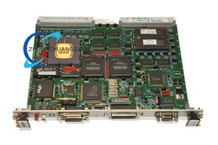
Board Material: Densan PCB laminate, connector plating and component finishes are confirmed only from the official board manual, not from component data alone.
Structural Characteristics
Integration: CPU, cache, DSP-class multiplier, DMA, timers, serial and interrupt hardware on one chip.
Bus Separation: Separate address, data, control and chip-select pins; PLL power pins isolated for noise reduction.
Peripheral Mapping: All on-chip peripherals accessed through memory-mapped registers.
Working Principle
The processor fetches 16-bit instructions into the five-stage pipeline, reads operands from 32-bit general registers, executes arithmetic, logic, multiply-accumulate or load/store operations, and writes results back to registers or external memory. Cache accelerates repeated access; DMA moves data between memory and peripherals without CPU load; timers and serial channels generate real-time events; the interrupt controller prioritizes external and internal requests; the bus controller converts CPU accesses into DRAM/SDRAM/flash control signals.
Installation Requirements
Power Decoupling: Place decoupling capacitors on every VCC/VSS pair and separate analog/PLL power planes.
Clock Circuit: Use the oscillator, crystal or external clock source defined by the board clock-mode strapping; allow PLL settling time before full-speed operation.
Reset Circuit: Provide clean power-on reset and manual reset with defined pulse width.
Memory Layout: Assign chip-select areas for SDRAM, flash and I/O devices before firmware initialization.
PCB Assembly: Follow QFP or BGA land patterns, reflow profile and inspection rules; BGA boards require X-ray or electrical continuity validation.
Usage Precautions
Electrical Limits: Never exceed absolute maximum supply and input ratings for the installed voltage grade.
NC Pins: Leave reserved and no-connect pins open unless the board manual defines their use.
Thermal Control: Maintain airflow or heatsinking so junction temperature stays within the qualified range.
ESD Handling: Use grounded workstations, wrist straps and anti-static packaging.
Safety Applications: Do not deploy in life-support, aerospace, nuclear or similar critical systems without written manufacturer qualification.





Reviews
There are no reviews yet.